NVIDIA's GeForce3: "NV20" Revealed
by Anand Lal Shimpi on February 27, 2001 9:16 AM EST- Posted in
- GPUs
Nothing more than a big Ultra?
 The
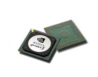
first thing to get over with the GeForce3 is that the 0.15-micron core, with
57 million transistors, has the same number of pixel pipelines and is clocked
at the same core speed as NVIDIA's GeForce2 GTS.
The reason for the die-shrink was to make room for the 128% increase in transistor count and to keep the GPU from eating too much power although we already expect it to run fairly hot. For those that don't remember, the GeForce2 GTS core was produced on a 0.18-micron fabrication process and boasted an incredible 25 million transistors. At 57 million transistors, the GeForce3 GPU is more complex than Intel's Pentium 4 processor in terms of sheer transistor count. Obviously this is a flawed comparison since the CPU guys have a much tougher job cramming in all the logic into as small and as efficient of an area, but it is a noteworthy parallel to make.
The GeForce3 still features the same four pixel pipelines that were present on the original GeForce 256 chip and two texture units per pipeline, a feature first introduced on the GeForce2 GTS.
The first advancement comes in the fact that the GeForce3 can now do single-pass quadtexturing. The GeForce 256 could use its four pixel pipelines to render four single textured pixels or two double textured pixels in a single pass, or a single clock. The GeForce2 GTS improved on this by adding a second texture unit per pixel pipeline, meaning that it could now render four dual textured pixels in a single clock. This is what gave the GeForce2 it's "Giga-Texel" moniker since it was now able to boast a peak fillrate of 1.6 Gtexels/s. However the Geforce2 is only capable of applying a maximum of two textures to a pixel in a single pass. The GeForce3 takes this one step further by now being able to do quadtexturing in a single pass, although it still has only two texture units per pipeline. This means that the GeForce3 can handle two quadtextured pixels in a single pass versus having to make two rendering passes in order to render the pixels. NVIDIA claims that this offers a theoretical peak fillrate of 3.2Gtexels/s although it seems like it's definitely time to stop quoting theoretical fillrate numbers in this industry.
The usefulness of this is incredible, to quote one of the industry's greatest developers, John Carmack, his experience with this feature of the GeForce3 was quite positive:
"An interesting technical aside: when I first changed something I was doing with five single or dual texture passes on a GF to something that only took two quad texture passes on a GF3, I got a surprisingly modest speedup. It turned out that the texture filtering and bandwidth was the dominant factor, not the frame buffer traffic that was saved with more texture units." - John Carmack, idSoftware
As for the memory clock of the GeForce3, it will be identical to that of the Ultra. Making use of the same 230MHz DDR SDRAM that debuted on the Ultra, the GeForce3 doesn't offer more raw memory bandwidth but an amount identical to that of the Ultra. This is still the greatest amount of raw memory bandwidth offered on any consumer level 3D graphics accelerator: 7.36GB/s.
This paints the picture that the theoretical fill rate of the GeForce3 is no greater than the previous generation of graphics chips from NVIDIA; if this were all the GeForce3 promised, we wouldn't be nearly as excited about this technology as we are. Keep on reading…


0 Comments
View All Comments